
Proof of Concept Demonstration
AgiLight is moving beyond the lab to show how its innovative laser technologies can make a real-world impact. Through a series of proof-of-concept demonstrations, the project will test its frequency-agile light sources in applications that matter to industry and society — from autonomous driving and infrastructure monitoring to marine exploration, quantum sensing, and environmental observation.
These demonstrations will showcase how AgiLight’s compact, fast-tunable, and ultra-stable lasers enable new levels of precision and performance. Field trials will include long-range 3D mapping with LiDAR, fiber-based sensing for structural safety, underwater imaging using blue light, quantum experiments for ultra-sensitive field detection and atomic clocks, and methane monitoring for climate applications.
By validating performance in realistic environments and collaborating with end users, AgiLight aims to accelerate the transition of its laser technology from research to practical solutions that shape the future of sensing, navigation, and environmental monitoring.
Light-source concepts and models
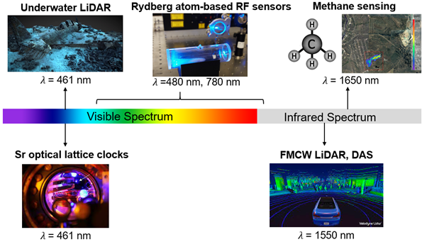
AgiLight aims to develop a new generation of laser sources covering wavelengths from the near-UV (400 nm) to the near-infrared (up to 2.7 µm), addressing a wide range of applications including underwater frequency-modulated continuous wave (FMCW) light detection and ranging (LiDAR) at 461 nm and quantum photonics experiments such as laser cooling of strontium atoms at 461 nm, Rydberg atom-based radio-frequency quantum sensors at 480 and 780 nm, optical coherence tomograpghy (OCT) at 960 nm, FMCW LiDAR at 1550 nm for autonmus driving, and environmental methane monitoring at 1650 nm. The “Light-Source Concepts and Models” pillar defines the core laser architectures and performance targets across this platform. It converts application requirements into tailored laser designs by selecting the most appropriate gain medium, feedback structure, and packaging strategy for each wavelength range. These elements work together to deliver stable, efficient, and compact light sources with unprecedented frequency agility and coherence. Through this systematic, application-driven design approach, each device concept is engineered for its target use case, thereby laying the foundation for subsequent technical project activities.
Tunable, Low-Loss Photonic Integrated Circuits
This pillar focuses on developing compact and energy-efficient photonic integrated circuits that can guide and control light with great precision. These chips are key to creating next-generation laser systems that are faster, more stable, and adaptable for various applications such as autonomous driving, precision sensing, and telecommunications. By improving how light interacts within these miniature circuits, we aim to make lasers more tunable while keeping energy losses extremely low.
So far, we made significant progress in advancing these technologies, successfully improveing the efficiency of materials that control light within these chips by nearly tenfold, allowing faster and more precise tuning. Ultra-low-loss waveguides have been developed that can carry light across a wide range of wavelengths —from blue to infrared— with minimal scattering, leading to much clearer and more stable laser outputs. We also designed and tested tiny circular resonators, known as microrings, that are essential building blocks for compact, high-performance lasers and optical frequency combs. New piezoelectric and electro-optic materials have been integrated into these chips, enabling light to be tuned more effectively through electrical control. Finally, the first generation of integrated chips for laser-based distance-sensing systems (LiDAR) has been fabricated and tested, showing very promising performance.
Together, these developments mark a major step toward creating compact, tunable, and reliable laser systems that could transform how light-based technologies are used in everyday life—from safer autonomous vehicles to faster communication networks.
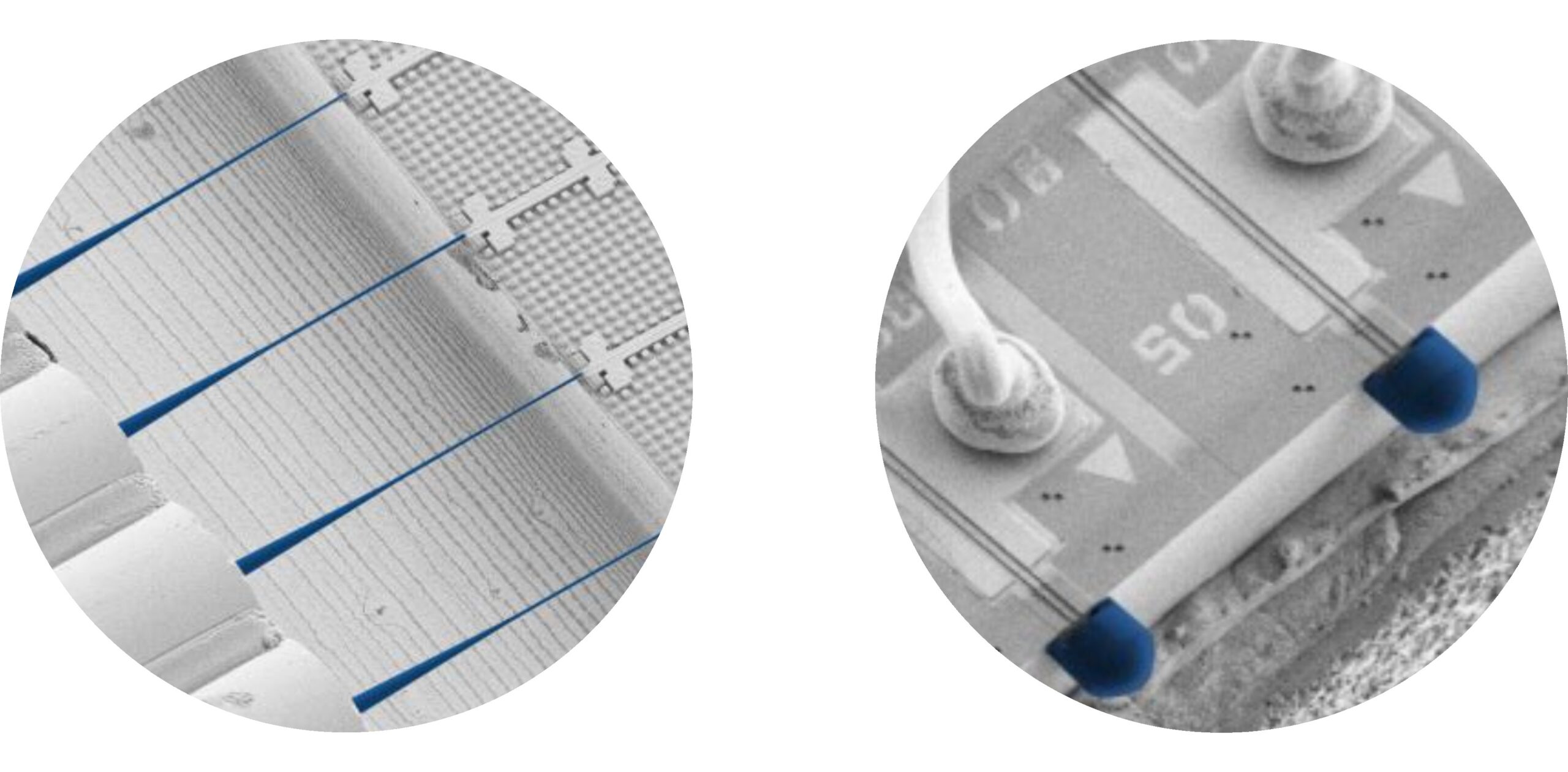
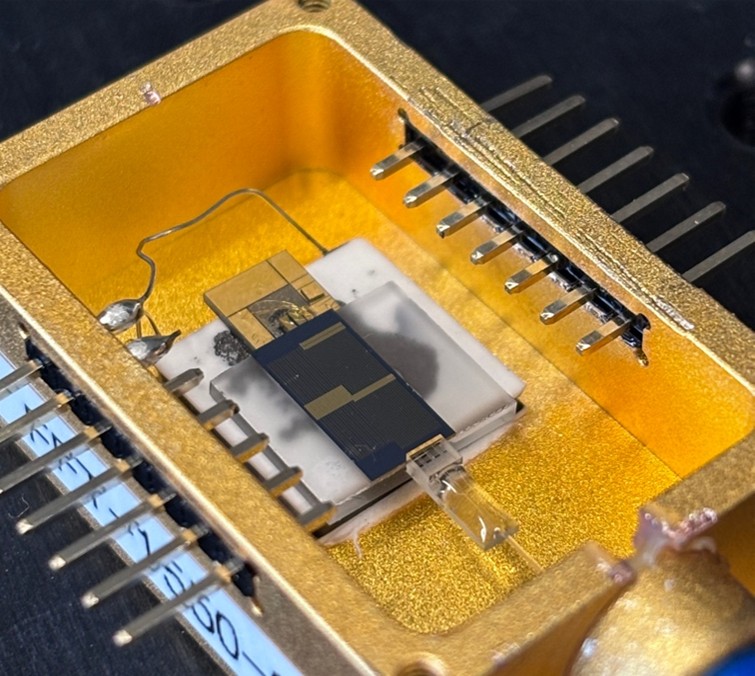
Laser Packaging
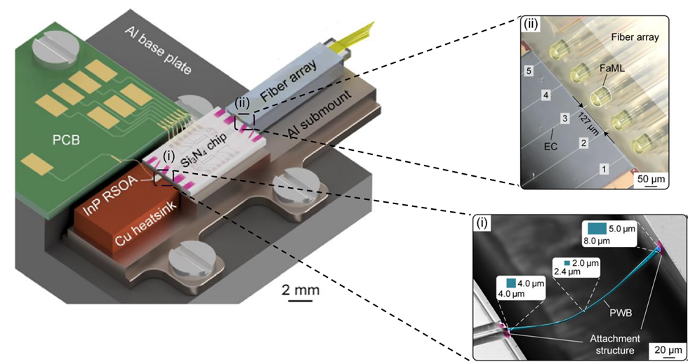
The hybrid integration concept envisaged in AgiLight crucially relies on low-loss package-level connections between the III-V-based gain element and the external-cavity feedback circuit. To provide the utmost flexibility and a clear path towards cost-efficient mass production, we will exploit 3D-printed coupling elements such as photonic wire bonds and facet-attached micro-lenses. VA has shown the capability for wafer-level processing, proving a clear path to industrialization. Along the same lines, we will explore the power resilience of such structures to support the envisaged intra-cavity power levels of AgiLight laser sources. Broadband 3D-printed chip-chip connections with power handling capabilities of 1 Watt do not exist today and will open an entirely new realm of hybrid photonic integrated circuits for high-power applications. For wavelengths beyond 1000 nm, we will use photonic wire bonds (PWB) or facet-attached microlenses (FaML). For wavelengths between 530 nm and 1000nm, we will rely on the newly developed FaML. Devices with shorter wavelengths in the blue or ultraviolet (UV) will predominantly be implemented by butt coupling and active alignment. At the same time, we will explore the potential of using FaMLs that are based on novel materials with low loss at low wavelength.